User Interview
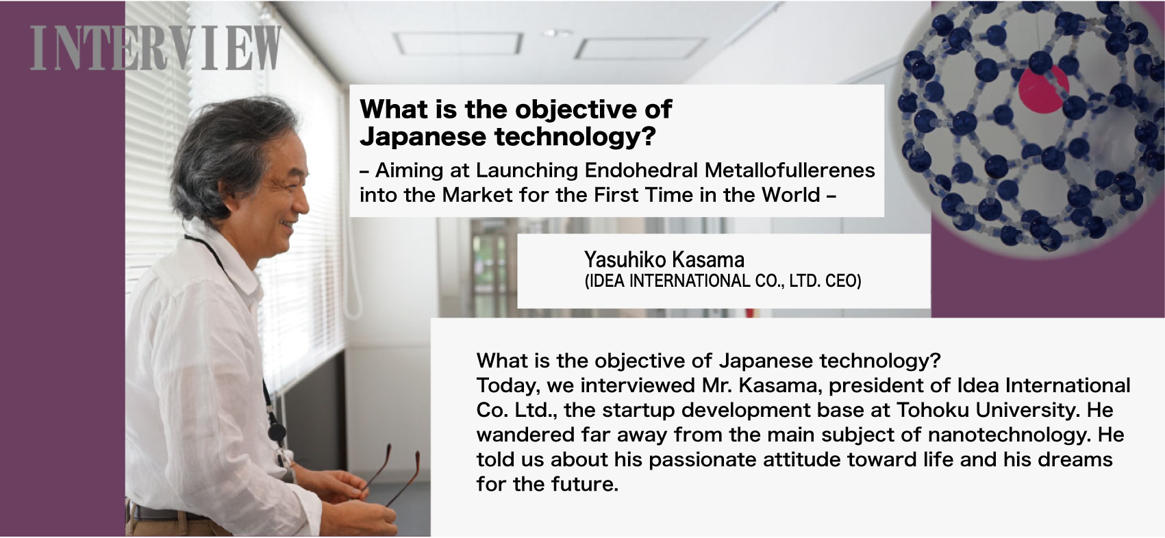
Today, we interviewed Mr. Kasama, president of Idea International Corporation, the startup development base at Tohoku University.
―What kind of business is the Idea International Corporation working on? ―
As a startup company, we have expanded the accumulated basic research by Tohoku University, which is leading to the development and industrialization of mass production technologies for endohedral metallofullerenes for the first time in the world. As new nanocarbon materials, lithium-ion-encapsulated fullerenes (Li+@C60) are expected to be used in a variety of different applications. One possibility is their use in flexible organic electronic devices like organic solar batteries, sensors, or accumulation devices.
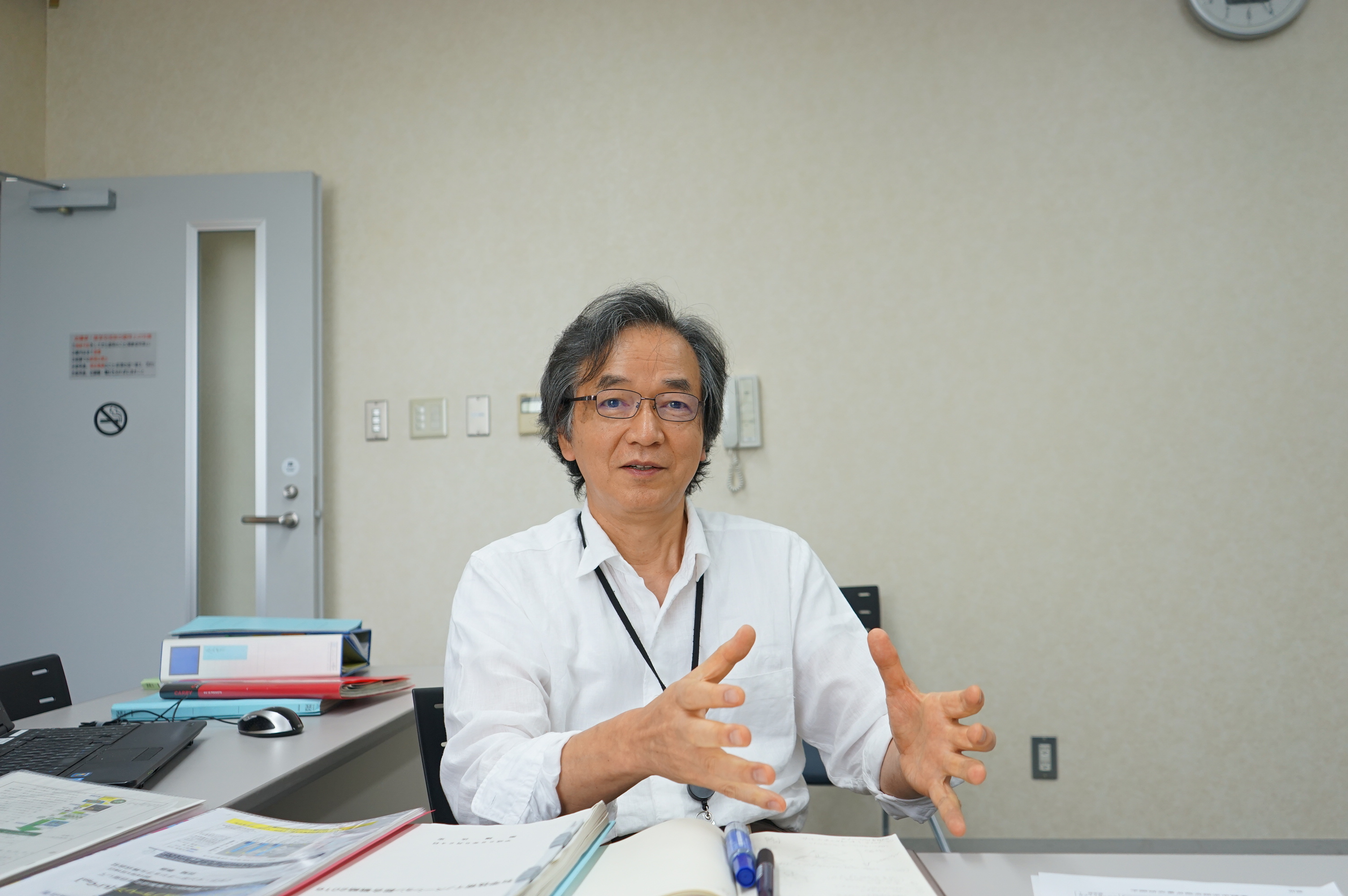
―Mr. Kasama, first, what inspired you to establish the startup?―
It’s a long story: originally, I worked at a major electronic parts manufacturer that developed high-definition liquid crystal displays. Back then, mainstream displays were cathode-ray tubes. However, I was interested in how fine we could make animage in order to satisfy people. Then, I understood that when people stared hard at an image and said that it looked just like a photo, it meant there was still more work to do. So, if it went beyond a picture? Based on that idea, I started a research and development joint venture with a company in South Korea by manufacturing equipment. On the other hand, I realized that the transmission and storage of information between the human eye and the brain were completely different from those on semiconductor devices, such as the current LSI.
― It sounds like things were going smoothly for you every day. Why did you quit your job? ―
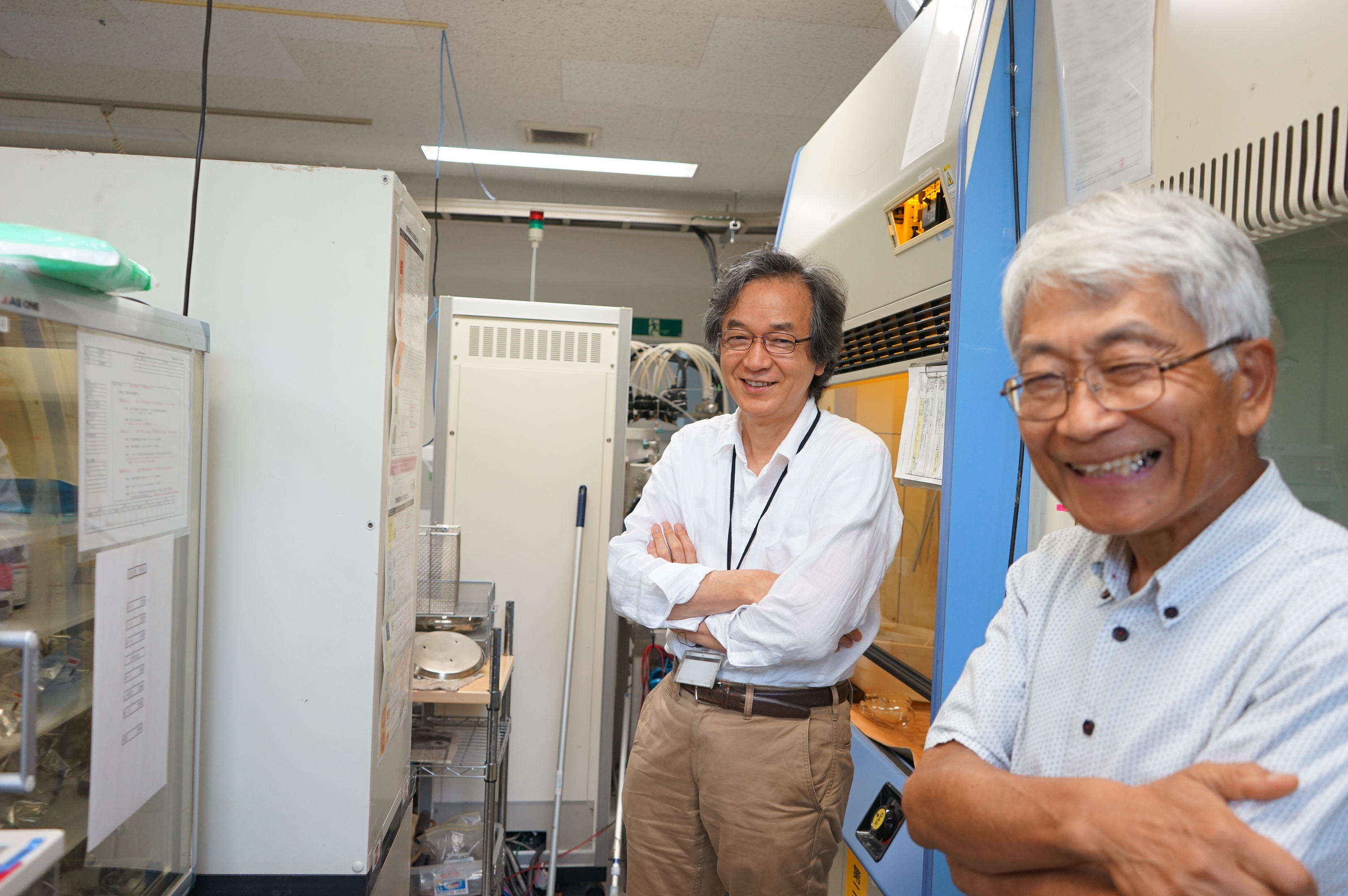
I had several reasons. However, the main reason wasthat I’d become keenly aware that the technical skills of manufacturers certainly started to decline, although Japan should have been a superior electronic-oriented country in the world. Since entering the company, I only saw things from the perspective of research and development. So I asked the company to let me see the actual manufacturing site once, and I was allowed to work inquality management. I had experienced how to respond to defects that occurred from our clients there. Our clients of electronic components are assembly manufacturers, that is, general electrical manufacturers. At the production site, there had already been delivery delays. So, some people tried to solve problems by force in an effort to try to decrease the loss. If the client-side loses an opportunity to launch a new model into the market, they will lose a business opportunity. So, they wouldn’t stay still but will try to find the cause of the defects by using a reasonably high-level of analytical equipment. However, it seemed that the farther you were from the manufacturing site, the farther you were from the defect phenomenon right in front of you. Even if you obtained data that was so good you could write a paper using the information, the data wouldn’t always lead to finding ways to solve the problems quickly. However, during this period, the defective products and human fatigue had just piled up one upon another at the manufacturing site. I picked up some defective products from the pile and conducted a screening test onthem. The screening test was conducted in a very direct (primitive) method. At that time, the people at the manufacturing site had been conducting the test manually and depended on physical strength. Then, I understood at once. The cause was not operations or designs at the manufacturing site, but defects during the manufacturing process of one important purchased part. A hair dryer and a tester were enough to prove this in front of everyone. To make doubly sure, I used an optical microscope image. Furthermore, I added a low-magnification scanning electron microscope (SEM) image. I took the images to the quality control department of a certain famous manufacturer in Kyushu Prefecture, which was manufacturing the component, and solved the problem. I don’t want to brag, but fortunately or unfortunately, I accidentally experienced a very similar phenomenon when I worked on a similar component from its development through production transfer. Let me take cell phones, for example, these days the manufacturing sites of many companies are engaged in processes from a lot of components and assemblies to the final products. To determine the real cause of defects in the final products, high-quality analysis equipment is not always immediately effective. Instead, the process to narrow down the cause of the defect from the defect phenomenon itself is important. I think optimal analysis equipment can prove the hypothesis. To do that, I think, it requires a specificlevel of understanding of system components and the manufacturing process. Everyone knows this, and it’s totally obvious. However, I felt that it started to weaken. The engineers’ world is a little strange. The colleague who helped me with the contrivance at that time was Kazuhiko Kawachi, that “old man with white hair (?).” He is engaging in the productivity improvement of Li+@C60 in the lab just now.
I gained experience in helping the development of a big company, as a small company employee, after I quit my job. The experience made me think about the positions of a big company and a startup. In the US, the core part of research and development is outsourced to startups. A big company and a startup have an equal relationship. Development is accelerated more efficiently in that way. The same is true for government commissioned research on advanced technologies. In Japan, however, hierarchical relationships tend to occur between the commissioning company and the commissioned company. That makes it difficult for startups to demonstrate their true worth. I thought you should make good use of startups for tasks of higher risk. I thought Japanese manufacturing might newly develop in this way in the future.
―You established as tartup pursuing your ideal, didn’t you? ―
There are many difficulties but the other day, my project was adopted by the NEDO.
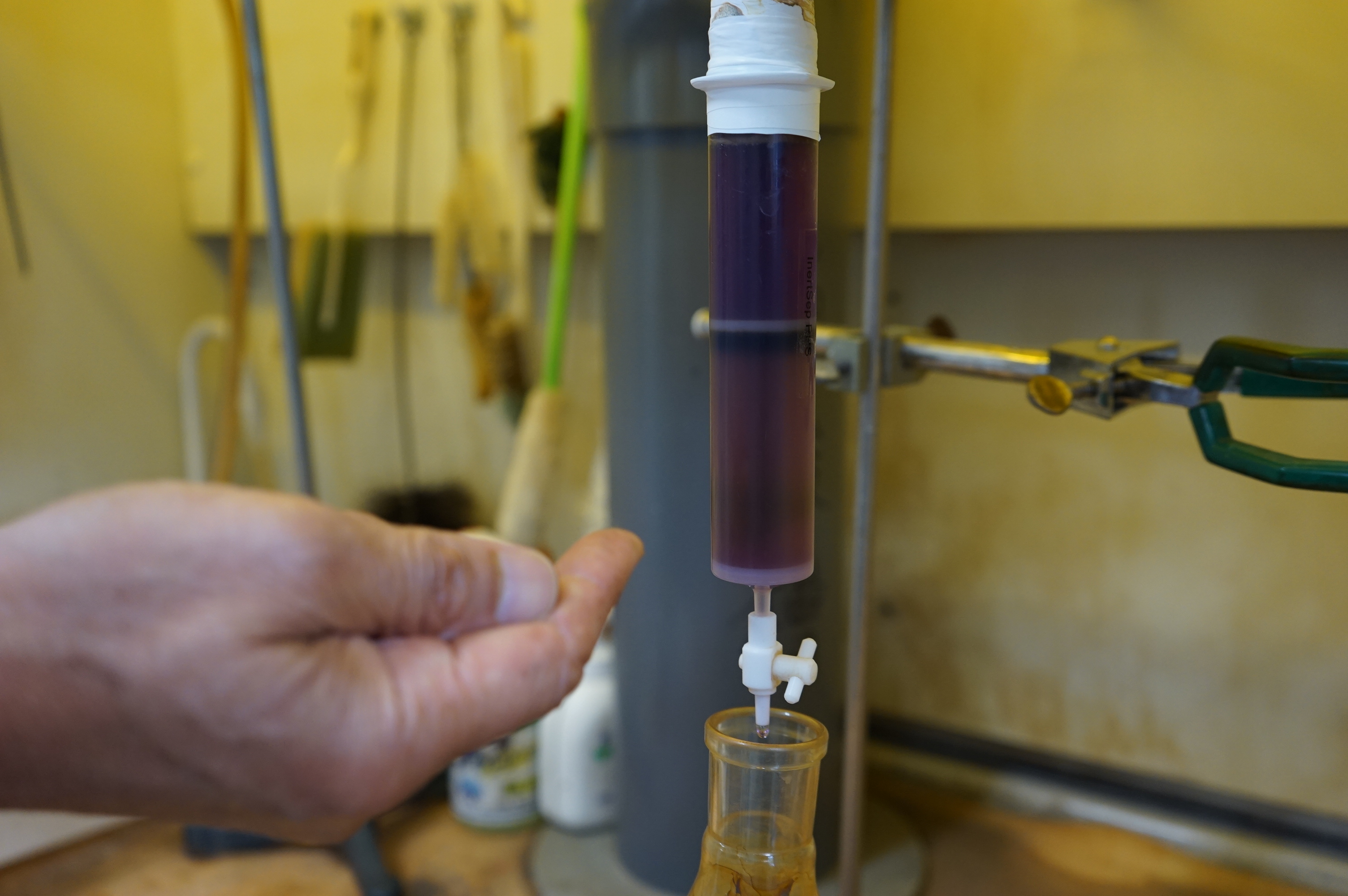
Currently, the productivity of Li+@C60 is on the order of tens of grams per year. This is an epoch-making number in aworld that handles atom-encapsulated fullerenes. In principle, we understand that we can achieve order-of-magnitude better productivity. In the future, I want to add one more piece of production equipment and decrease the price to allow more researchers to use us.
Think of the Balance Between the Profit of Companies and Research by Universities
Provide a Place for Interdisciplinary Research Including Startup Companies
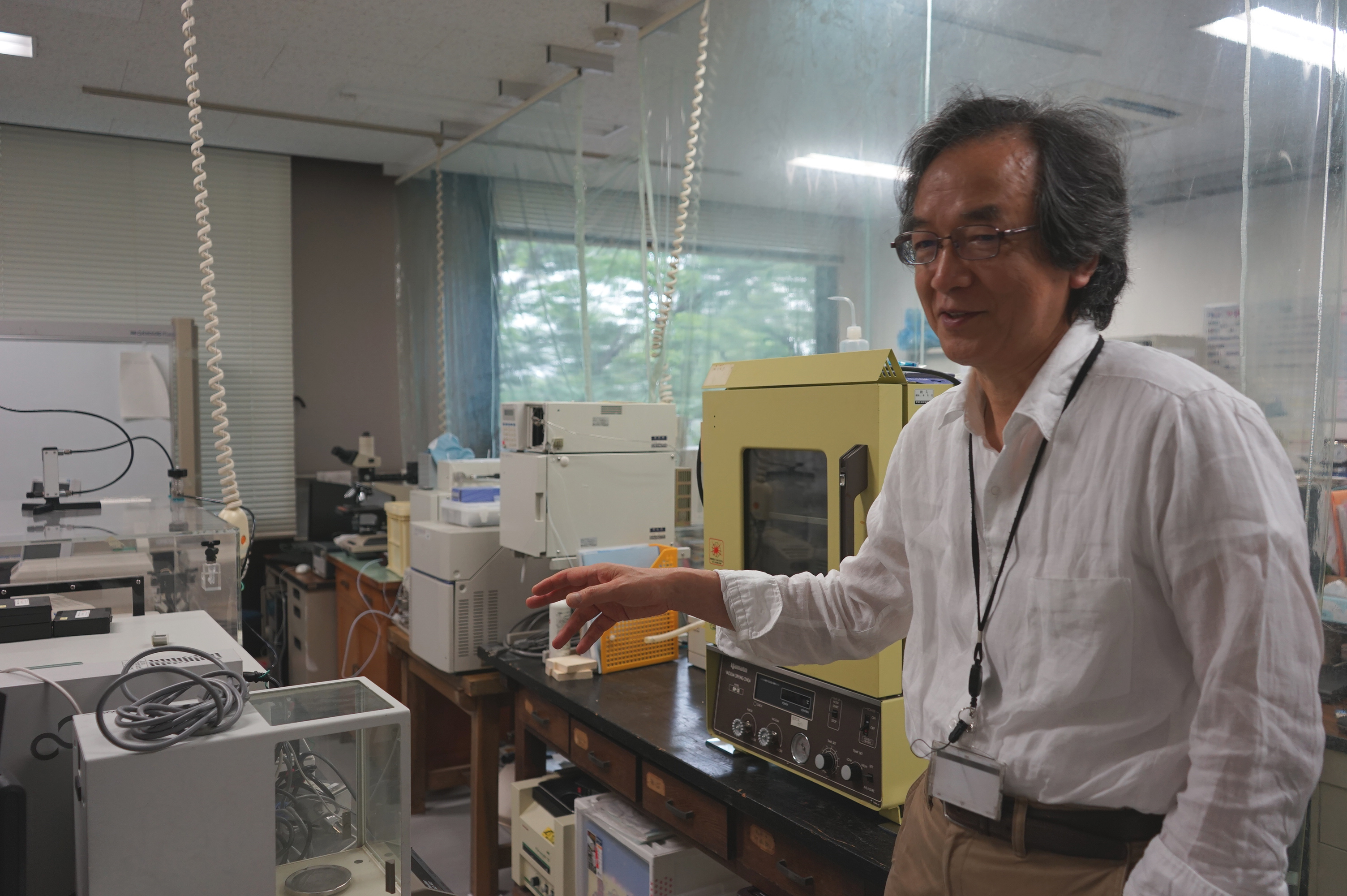
―Finally, I’d like to hear about how you are using the Nanotechnology Platform. ―
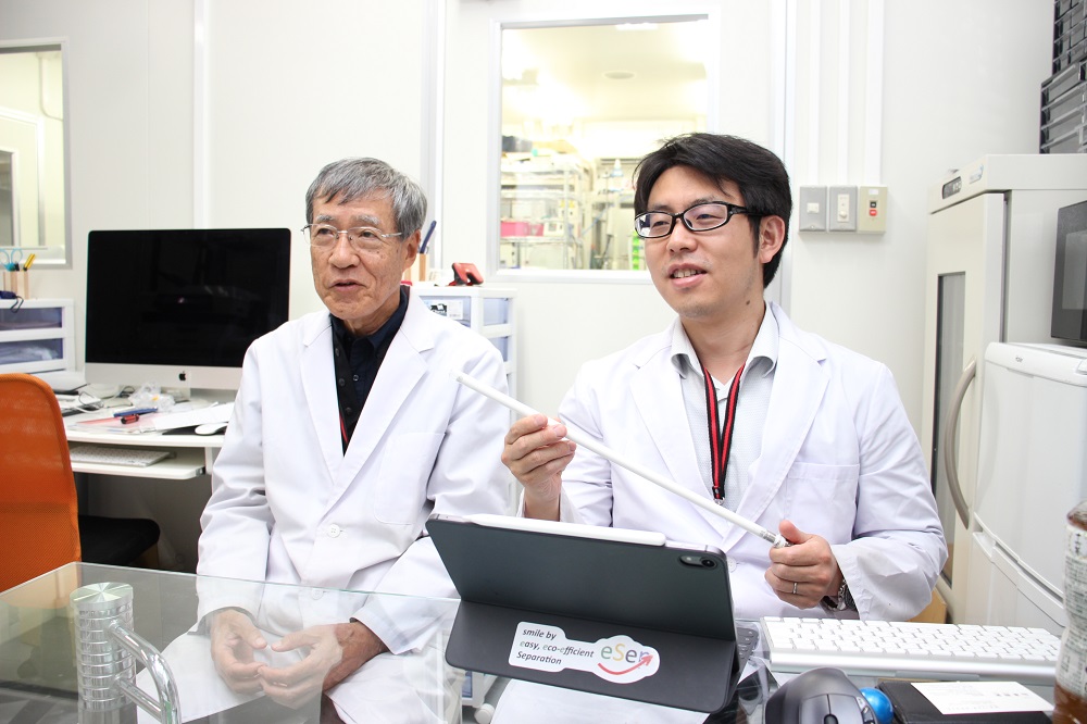
First of all, when we were working on nanotechnology, especially on the substance Li+@C60, which is not available to anyone yet, Kwon Eunsang, an associate professor at the Research and Analytical Center for Giant Molecules, Graduate School of Science, Tohoku University, led us to the Nanotechnology Platform. Our company would not even exist without him. That’s because he is supporting us not only in equipment usage but also in a wide variety of other fields with his knowledge and wisdom based on a wide range of academic perspectives. In addition, NMR is very easy to use. The staff respond quickly to us if they are available. Being able to carry out research and development without being restricted by a lack of equipment makes it possible to achieve effective process development, resulting in a substantial reduction in the cost of products. Furthermore, we established good relationships with the teaching staff and departments at Tohoku University through Associate Professor Kwon Eunsang. I will keep growing more by effectively using the exact platform where knowledge, equipment and human resource are all available.
Back Number


Molecule and Material Synthesis Platform
National Institutes of Natural Sciences Institute for Molecular Science
38 Nishigo-Naka,Myodaiji, Okazaki 444-8585, Japan
TEL +81-564-55-7447