User Interview
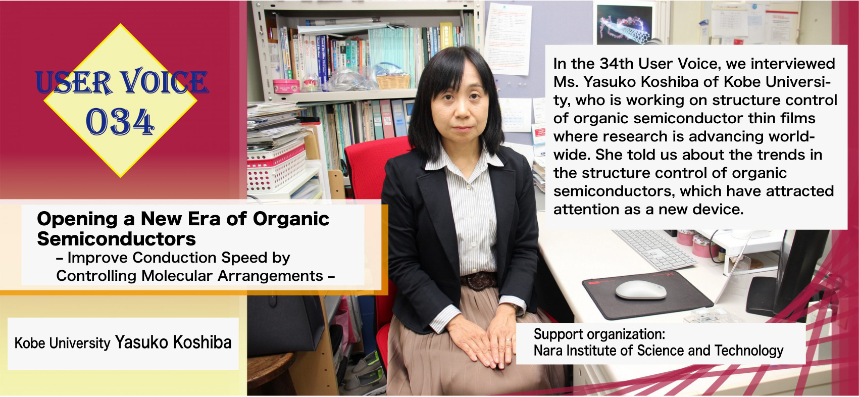
Create Crystals Where Molecules are Aligned
―You have been doing research on structure control and the evaluation of the function of organic semiconductor thin films with the objective of applying it to devices since being in school, haven’t you?
When I was a student, the term organic semiconductor was not as common as it is today. After graduation, I left the research profession for a time and started working at a chemical company. But I became involved in the research of organic semiconductors about 15 years ago. Currently, I am evaluating the nanoscale structures of organic semiconductors like phthalocyanine. At the same time, I am trying to establish doping technology in the organic semiconductors with the goal of applying this to devices, including photodetectors and thermoelectric conversion elements.
―It is said that the structure control of thin films is important.
The structure of organic molecules presents anisotropic properties, so the structure control of thin films is important. I believe that by adopting the three-dimensional rod structure, the wider surface area will receive light even when the same amount of light falls on the area. Furthermore, if the molecules of crystals are fully aligned, carriers conducting electricity can move quickly. So, I am trying to obtain crystals where the three-dimensional rods are aligned as fully as possible. In addition, the method of crystal production is different depending on the molecule. I am performing the vacuum evaporation technique where the molecules are dispersed in a vacuum and deposited on a substrate to make thin films. If you do nothing, it only becomes granular. So I am investigating the conditions required for vapor deposition. I believe that forming rods is largely involved in molecular orientation.
Change the Electronic State by Doping
―You focused on the electronic state.
In order to accelerate the carriers, the electronic state is important. Organic semiconductor materials change their electronic state by doping. That is, performance will change. For example, conductive polymers change electrical conductivity depending on the state of oxidation. For use as electrodes, high electrical conductivity is suitable. For thermoelectric conversion materials, decrease the electrical conductivity. I am controlling doping levels to achieve optimum value. However, it requires time to control everything.
Prepare Samples at the Nara Institute of Science and Technology
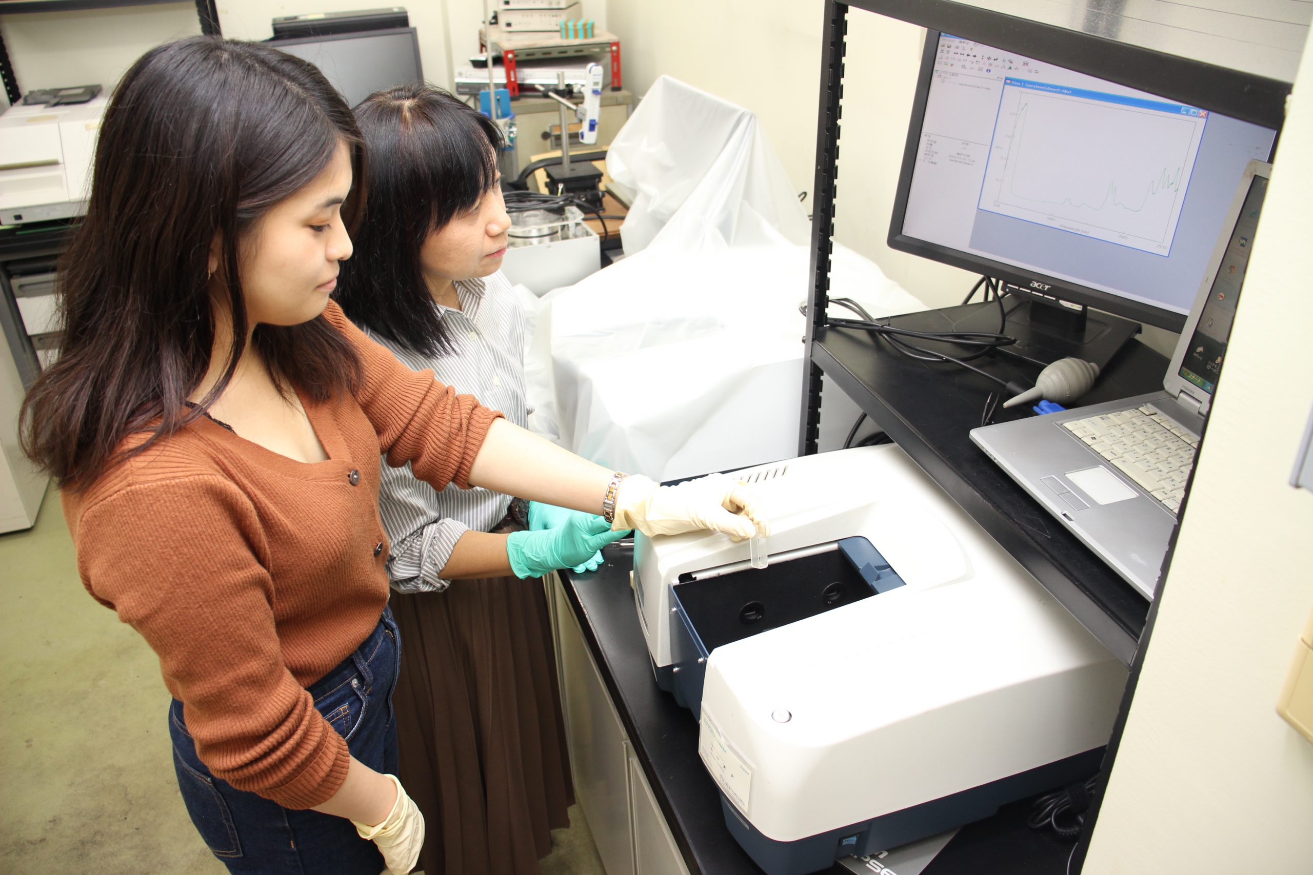
―How did you feel when you used the Nanotechnology Platform project?
I’ve used the platform since 2015. It is helpful because I can use the equipment necessary to advance the research. For example, I used a photoelectron spectrometer for measuring the ionization potential in the changes in the electronic state according to the deposition conditions of thiophene-based material films. I can use AC-2 type equipment at Kobe University as well. However, the Nara Institute of Science and Technology has the AC-3 type, so I was able to obtain data from a wider measurement range.
―You prepared samples at the Nara Institute of Science and Technology, didn’t you?
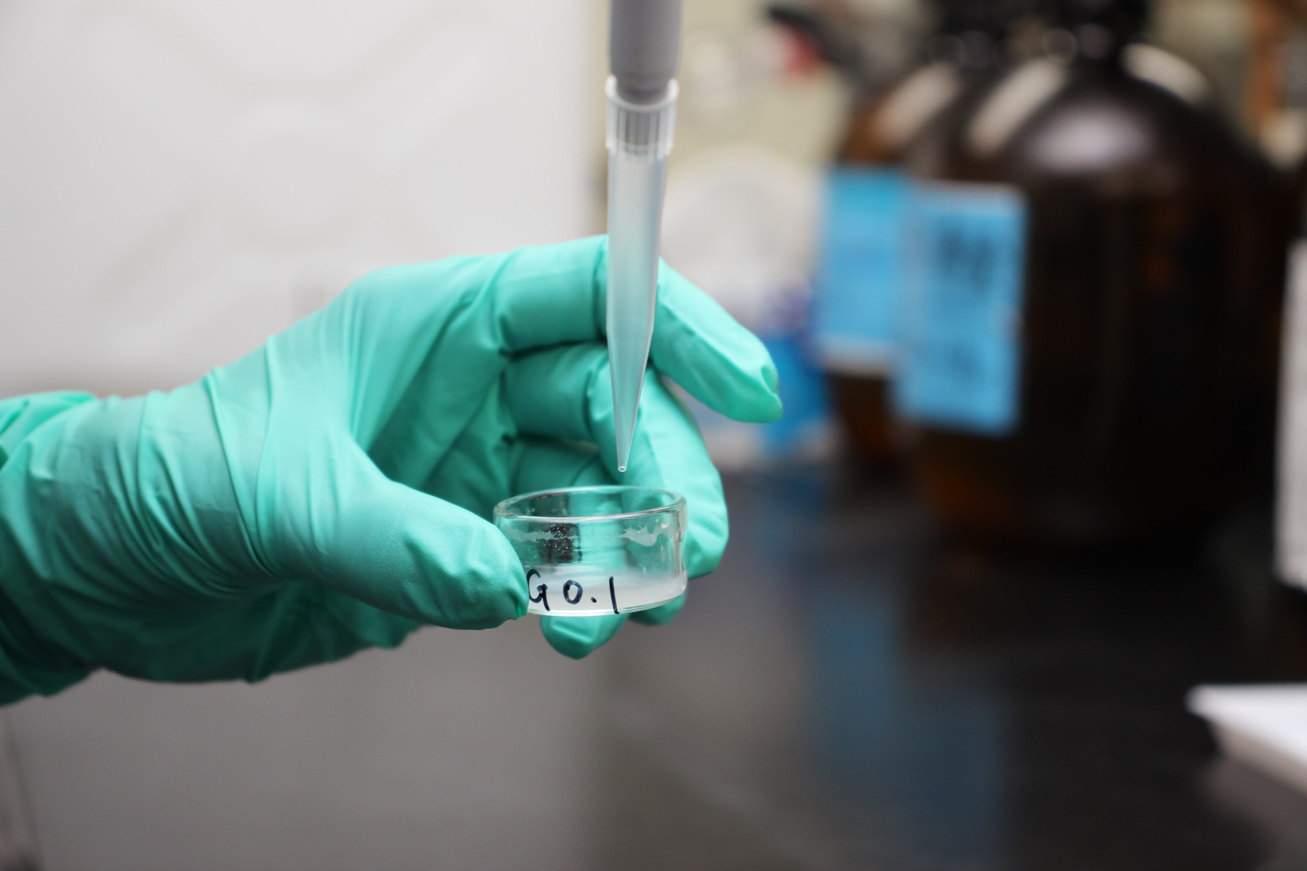
The experiment was about doping levels. If the material was not measured just after the doping, the characteristics of the material would change. So, I was allowed to use a laboratory with the support of Mr. Yoshiyuki Nonoguchi, and I prepared samples for two days. I was not able to carry the samples; nevertheless, they obtained internal consensus within the university before I went there so that I could carry on my experiments without any problems. That really reassured me. In addition, technical personnel have a high level of technical knowledge of the equipment. So I knew of the method’s disadvantages, sample preparation methods, and the latest information.
STEM Allow You to Switch Between TEM and SEM
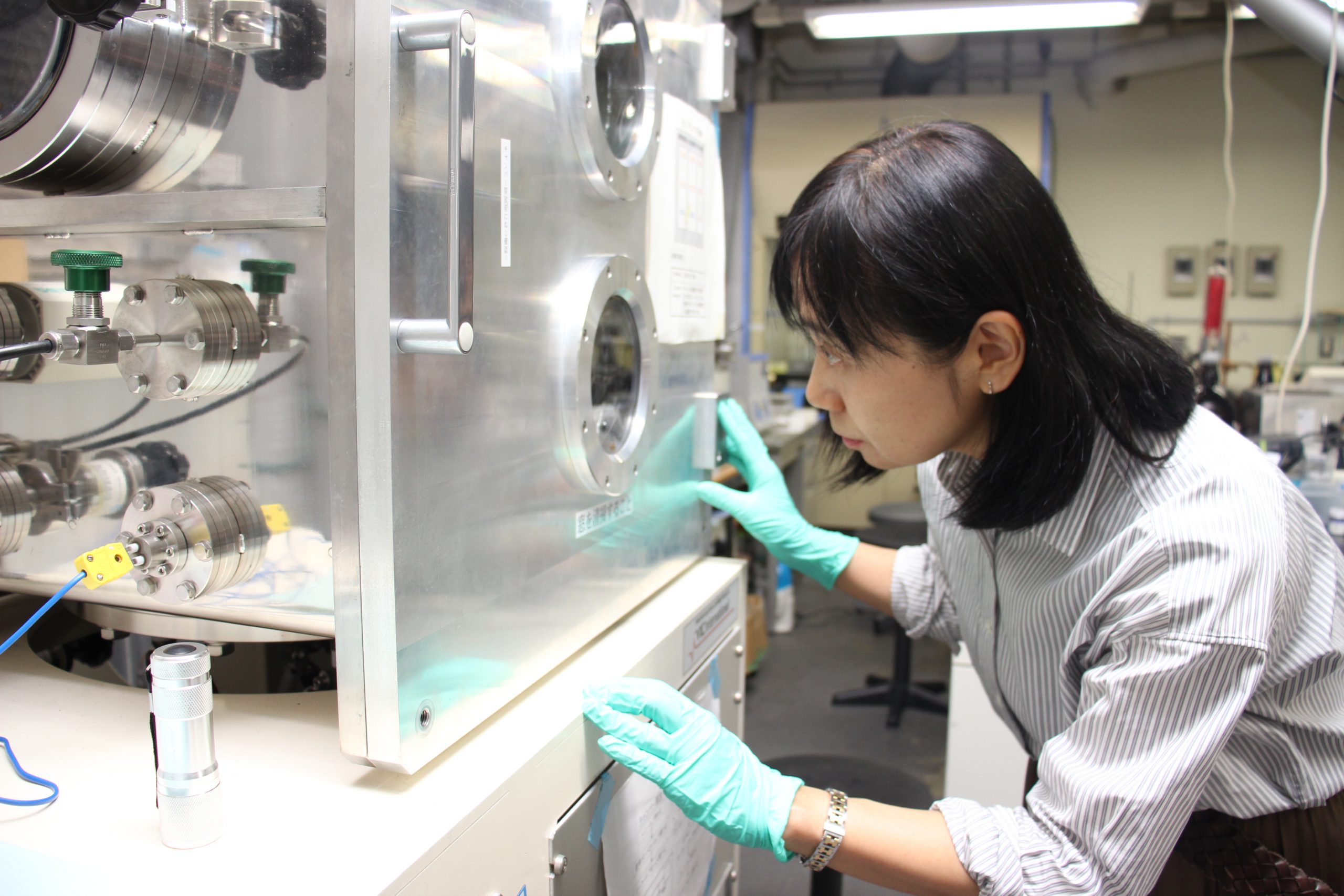
―You used a scanning transmission electron microscope (STEM) to observe the nanorods.
Yes, I did. It is difficult to prepare samples for STEM, so I was sometimes not able to observe them at all. We should observe each nanorod, so I made every effort to ensure that we achieved the optimal dispersion. One of the best characteristics of this STEM is being able to switch between the transmission electron microscope (TEM) and the scanning electron microscope (SEM). Doing that is a significant advantage when you can observe TEM and SEM images of the same sample without changing the visual field. I also obtained information on the overlap of nanorods and the existence of metallic elements. I think it is difficult for all universities to purchase expensive equipment. If each university shares equipment, it can support researchers in trouble due to the lack of the necessary equipment. I hope that this project will continue.
Back Number


Molecule and Material Synthesis Platform
National Institutes of Natural Sciences Institute for Molecular Science
38 Nishigo-Naka,Myodaiji, Okazaki 444-8585, Japan
TEL +81-564-55-7447